Everyone talks about ChatGPT, Gemini, and Claude. The headlines celebrate the software, the prompts, and the benchmark scores. But none of these AI models would exist – or respond as fast as they do – without a tiny piece of hardware that almost nobody talks about: High Bandwidth Memory (HBM). This week, Samsung shipped the most advanced version ever manufactured: the 12-layer HBM4E. Here is everything you need to understand about why this matters, and what it means for the AI tools you use every day.
What Exactly Is HBM and Why Does AI Need It?
To understand why HBM4E is a big deal, you need to understand the fundamental bottleneck in AI computing. When a large language model like GPT-5 or Claude generates a response, it is performing billions of mathematical operations per second. Each of these operations requires pulling data from memory and sending results back – constantly, at enormous scale.
Traditional DRAM memory (the kind in your laptop) uses a narrow pathway to transfer data – imagine a single-lane road. It works fine for everyday computing. But for AI, it is like trying to funnel a river through a garden hose. The processor is left waiting, starved of the data it needs. This is the "memory-bandwidth bottleneck," and it is the single biggest hardware constraint in AI today.
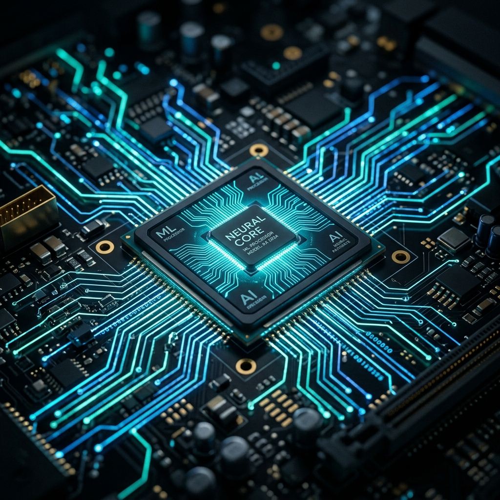
High Bandwidth Memory solves this by physically stacking multiple layers of memory chips on top of each other, connected by thousands of microscopic vertical pathways called Through-Silicon Vias (TSVs). Instead of one lane, you get thousands of parallel lanes moving data simultaneously. The "12-layer" in Samsung's HBM4E literally means 12 memory dies stacked vertically – each one connected to the next by those microscopic through-holes.
The HBM4E Numbers That Actually Matter
Here are the key specifications for Samsung's new HBM4E, and what each one means in practical terms:
- Bandwidth: 3.6 TB/s per stack – A 20%+ improvement over the previous HBM4 standard. This means 3.6 terabytes of data can flow through a single memory stack every second. For context, that is roughly equivalent to transferring the entire text of Wikipedia in under one millisecond.
- Capacity: 48GB per stack – With 32GB and 64GB variants already in development. Larger capacity means AI models can hold more of their parameters in fast memory, reducing costly trips to slower storage.
- Pin Speed: 14–16 Gbps – A new industry benchmark that pushes the theoretical limits of current packaging technology.
- Energy Efficiency: 16% improvement – Critical for data centers where electricity costs are the primary operational expense. More efficient chips mean lower API costs for end users.
- Thermal Performance: 14% better heat resistance – AI chips generate enormous heat. Better thermal performance means higher sustained performance without throttling.
Why Samsung Shipped Early – The Competitive War Behind the Headlines
Samsung originally scheduled HBM4E for a mid-2026 release but accelerated the timeline by months. This was not an accident. The AI memory market has become the most brutally competitive segment in the entire semiconductor industry, and Samsung was losing.
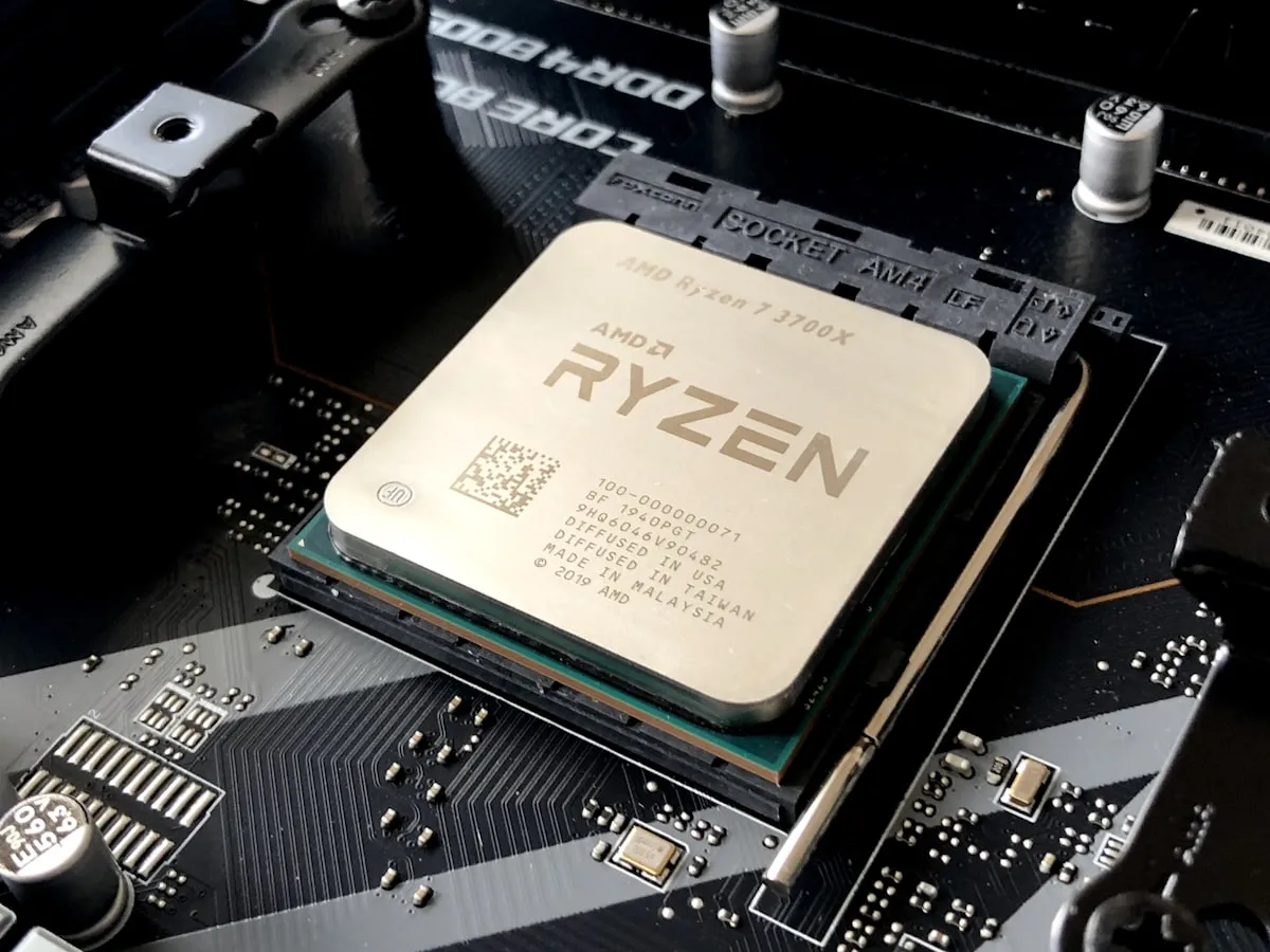
For two consecutive years, their South Korean rival SK Hynix dominated the HBM market, capturing the majority of orders from Nvidia – the primary customer for HBM chips. Nvidia's H100 and H200 GPUs, which power most of the world's AI data centers, ran almost exclusively on SK Hynix memory. This was both a massive revenue loss and a significant reputational blow for Samsung.
Samsung's early shipment of HBM4E is a clear, aggressive signal: they are done playing catch-up. They are competing to be the first choice for Nvidia's next-generation Blackwell Ultra and Rubin GPU architectures. For consumers and AI companies, this fierce competition is excellent news. When Samsung and SK Hynix race to out-innovate each other, the industry benefits from faster performance at lower prices.
The Hidden Bottleneck Nobody in AI Talks About
Here is a reality that most AI coverage misses entirely: the biggest bottleneck in AI inference (when a model generates a response) is not the processor, not the algorithm, and not the training data. It is memory bandwidth.
Large language models are "memory-bound" workloads, meaning the GPU spends more time waiting for data from memory than it does actually computing. Every significant improvement in HBM bandwidth directly and immediately translates into three things you actually care about:
- Faster AI responses – ChatGPT, Claude, and Gemini become noticeably quicker at generating text and reasoning through complex problems.
- Larger context windows – With more bandwidth and capacity, models can process longer documents, more complex code, and more extended conversations without hitting limits.
- Lower API costs – When the same hardware processes more requests per second, the per-query cost drops, which eventually filters down to consumer pricing.
How HBM4E Compares to Previous Generations
| Specification | HBM3E | HBM4 | HBM4E (New) |
|---|---|---|---|
| Bandwidth | 1.15 TB/s | ~3.0 TB/s | 3.6 TB/s |
| Max Capacity | 24GB | 36GB | 48GB+ |
| Layers | 8-layer | 8–12 layer | 12-layer |
| Pin Speed | 9.6 Gbps | 12 Gbps | 14–16 Gbps |
What This Means for You in the Next 12–18 Months
You will never purchase an HBM4E chip personally – they cost tens of thousands of dollars and are sold exclusively to companies like Nvidia, AMD, and Google. But the effects will reach you directly:
Within the next year to eighteen months, the AI tools you use daily – writing assistants, image generators, code helpers – will become measurably faster and more capable. Tasks that currently require breaking up a long document into chunks will work seamlessly with full documents. AI assistants will maintain longer, more coherent conversations. And if history is any guide, fierce HBM competition between Samsung and SK Hynix will help keep cloud AI pricing competitive.
The AI revolution is not just built by software engineers writing code. It is built in semiconductor fabrication plants in South Korea, by engineers who spend their careers stacking silicon wafers layer by microscopic layer, each one bringing the technology one step closer to what comes next.
? Frequently Asked Questions
?? Related Articles


Founder of AI Profit Hub. I explore AI tools, test them hands-on, and break down complex technology into practical, actionable guides. My goal is to help you work smarter using the best AI has to offer.