South Korea's $576 Billion AI & Semiconductor Master Plan: Samsung and SK Hynix Lead the Global Race
⚡ Key Takeaways
- South Korea announced $576 billion+ in AI and semiconductor investments — the world's most ambitious national tech plan
- Samsung and SK Hynix will build 4 new memory fab plants in the southwestern region
- SK Hynix controls ~60% of the global HBM market — the critical memory chip powering AI systems
- LG Electronics launched a Robotics Business Center on July 1, 2026 — adopting 10,000 NVIDIA GPUs
- AI data center targets: 550 trillion won by 2029, scaling to 1,000 trillion won by 2035
- Strategic "triple axis": semiconductors + Physical AI + AI data centers
📋 Table of Contents
- The $576 Billion Plan: Overview
- Samsung & SK Hynix: Building the World's Chip Backbone
- HBM: The Memory Chip at the Heart of AI
- LG Electronics' Physical AI Pivot
- AI Data Centers: Korea's Infrastructure Moonshot
- Risks, Analyst Concerns, and the Overcapacity Question
- Global Context: Korea's Place in the AI Chip Wars
- FAQ
On June 29, 2026, South Korean President Lee Jae Myung stood before the nation's top technology executives and announced what may be the most ambitious national technology investment program in human history: a sweeping, multi-decade plan totaling over $576 billion in coordinated public and private investment, targeting AI semiconductors, physical robotics, and AI data center infrastructure.
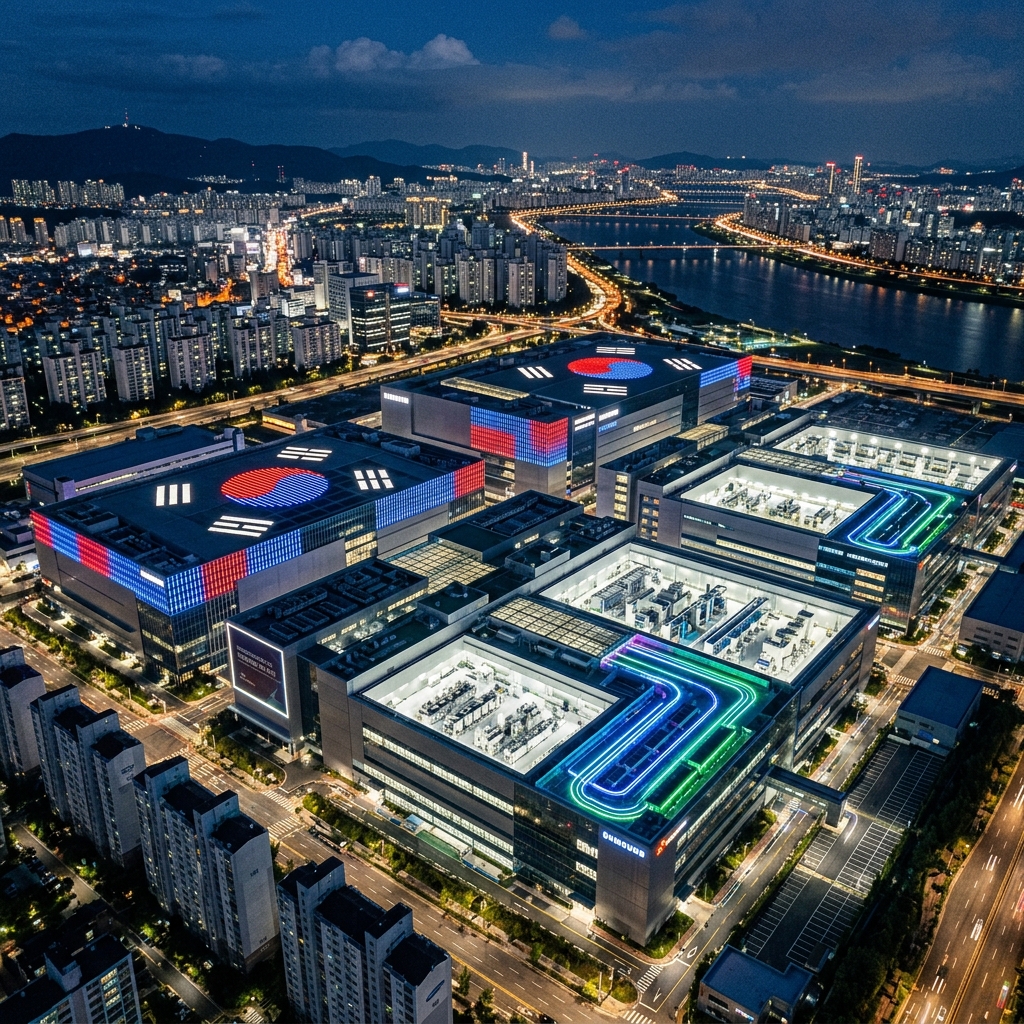
At the center of the plan stand Samsung Electronics and SK Hynix — the world's two largest memory chipmakers — committing to a joint investment of approximately 800 trillion won (~$518 billion) for new fabrication plants. With this announcement, South Korea is not merely defending its existing semiconductor leadership; it is making a generational bet that the AI era will require a 10x increase in advanced memory production, and that no country is better positioned to supply it.
The $576 Billion Plan: Overview and Strategic Logic
President Lee's announcement frames the investment around what he calls the "triple axis" of Korea's competitive future: semiconductors (the physical hardware of AI), Physical AI (robots and autonomous systems), and AI data centers (the cloud infrastructure that runs AI services). Each axis reinforces the others, creating an integrated industrial ecosystem that no single country currently possesses at this scale.
The plan also reflects a geopolitical dimension: President Lee has explicitly framed decentralization of South Korea's industrial base — long concentrated in the Seoul metropolitan area — as a core goal. The new semiconductor fabs will be built in the southwestern region, while the chip packaging cluster goes to Chungcheong. This regional industrial policy aims to distribute the AI economy's benefits more broadly across the country.
Beyond the fab investments, Samsung, SK Hynix, and partner firms have pledged an additional 392 trillion won (~$253 billion) for projects in the Chungcheong region, covering HBM chips, AI server components, next-generation displays, and battery technology — ensuring that Korea's AI supply chain extends well beyond memory chips into the full hardware stack.
Samsung & SK Hynix: Building the World's Chip Backbone
Together, Samsung and SK Hynix produce roughly two-thirds of the world's memory chips. Their coordinated commitment to this investment plan is unprecedented in scale — and reflects both the enormous demand signals coming from AI hyperscalers globally, and the strategic pressure to maintain Korean leadership as Chinese competitors like CXMT rapidly scale their own DRAM production.
Samsung's investment priorities center on advanced DRAM and next-generation packaging technologies that enable the dense, high-bandwidth memory configurations required by AI training clusters. The company has faced competitive pressure from SK Hynix in the HBM segment specifically — a situation the new investment aims to remedy through dedicated HBM production lines.
SK Hynix, meanwhile, is pressing its advantage. Beyond the national investment commitment, SK Hynix announced its own $64.4 billion capital plan that includes a new NAND flash factory (designated M17) scheduled to break ground in 2027, and a new advanced packaging facility (P&T7) already under construction in Cheongju. The packaging facility is particularly significant: advanced packaging — the process of stacking and connecting chips at microscopic scale — is increasingly where competitive differentiation in AI chips is won or lost.
HBM: The Memory Chip at the Heart of AI
High-Bandwidth Memory (HBM) has emerged as one of the most strategically important components in the global AI supply chain. Unlike traditional DRAM, HBM stacks multiple memory dies vertically and connects them through thousands of microscopic channels, delivering data to AI processors at speeds 10–15x faster than conventional memory — a critical requirement for training large language models efficiently.
SK Hynix currently commands approximately 60% of the global HBM market — a position it established by supplying HBM3E chips to NVIDIA for its H100 and H200 GPU series, which power the majority of the world's AI data centers. This dominance has been the primary driver of SK Hynix's valuation surge over the past 18 months.
The South Korean government's goal of doubling domestic DRAM production within five years is explicitly designed to ensure that HBM supply can scale in proportion to AI demand — which analysts project will grow at 30–40% annually through the decade. For AI companies globally, South Korea's investment plan is not just an economic story; it is a supply chain security story that directly affects the pace at which AI can be deployed at scale.
LG Electronics' Physical AI Pivot: From Appliances to Robots
On July 1, 2026 — the same day the national investment plan began formal implementation — LG Electronics made a structural change that signals its strategic transformation: it established a Robotics Business Center reporting directly to the CEO, bypassing the traditional divisional hierarchy.
This move reflects LG's explicit repositioning as a "Physical AI" company — a term increasingly used to describe enterprises that embed AI directly into physical machinery, manufacturing, and logistics. LG is deepening its partnership with NVIDIA, reportedly adopting 10,000 NVIDIA GPUs to train AI systems for its robotics division, smart factory solutions, and data center cooling businesses.
Industry analysts have begun modeling LG's robotics revenues separately from its traditional appliance business, a recognition that the two units are increasingly divergent in their growth trajectories. LG is also expanding into ASIC (Application-Specific Integrated Circuit) design services — a move that would position it as both a customer and a supplier in Korea's semiconductor ecosystem. For a company historically known for washing machines and televisions, this transformation represents one of the most dramatic strategic pivots in Korean corporate history.
AI Data Centers: Korea's Infrastructure Moonshot
Chips alone do not create an AI economy — they must be housed, cooled, and connected in data centers that can operate at extraordinary scale. The South Korean plan explicitly targets 550 trillion won in AI data center investment by 2029, scaling to over 1,000 trillion won by 2035. These are not aspirational figures; they are anchored by specific commitments from Samsung, SK Hynix, and a coalition of domestic cloud and technology companies.
Korea's data center ambitions are supported by several structural advantages: a highly reliable power grid, advanced telecommunications infrastructure (Korea has the world's highest 5G penetration rate), and a dense concentration of semiconductor expertise that reduces the technical complexity of building AI-optimized facilities. The country is also developing innovative cooling technologies, drawing on LG's HVAC expertise — a convergence of its traditional manufacturing competency and its new AI focus.
Risks, Analyst Concerns, and the Overcapacity Question
Not all observers are uniformly enthusiastic. Several prominent equity analysts have flagged the risk of AI chip overcapacity — a scenario in which memory production outpaces demand, leading to price collapses similar to those seen in the DRAM market during 2023–2024. If global AI adoption decelerates or if novel chip architectures reduce per-workload memory requirements, the economics of the multi-hundred-billion-dollar investment could deteriorate rapidly.
Minority shareholders at both Samsung and SK Hynix have requested greater transparency on how these capital commitments will affect future dividends and free cash flow. The concern is legitimate: building four new semiconductor fabs requires years of construction before generating revenue, and capital tied up in construction cannot be returned to shareholders or deployed into faster-growing opportunities. The government's strategic framing of this as "essential national infrastructure" does not eliminate the financial risk for individual investors.
Global Context: Korea's Place in the AI Chip Wars
South Korea's $576 billion plan does not exist in isolation. It is part of an accelerating global race for AI hardware supremacy. The United States is investing hundreds of billions through the CHIPS Act and private sector commitments from Intel, TSMC, and Samsung's US fab in Texas. Japan, through its Rapidus initiative and the newly announced Noetra consortium, is investing over $10 billion in domestic AI chip and Physical AI capabilities. China, despite US export restrictions, is channeling massive capital into Huawei's Ascend architecture and SMIC's chip manufacturing.
In this context, South Korea's investment is best understood not as an act of corporate ambition but as a national survival strategy. The country's economy is more dependent on semiconductor exports than any other major economy — semiconductors represent approximately 20% of South Korea's total exports. If AI-driven demand for advanced chips proves as sustained and large as projections suggest, Korea's existing leadership in HBM and DRAM positions it for extraordinary economic growth. If those projections prove too optimistic, the country faces the risk of having committed an extraordinary share of its national wealth to a cyclical industry at its peak.
❓ Frequently Asked Questions
📚 Sources & References
- Tom's Hardware — South Korea $576B Semiconductor Investment Plan (June 2026)
- Financial Times — Samsung and SK Hynix Commit to New Fabs
- Bloomberg Technology — SK Hynix HBM Market Dominance Analysis
- Reuters — LG Electronics Robotics Business Center Launch
- Straits Times — Korea AI Data Center Investment Targets 2029–2035

AI Profit Hub Editorial Team
Our editorial team comprises AI researchers, tech journalists, and industry analysts with expertise spanning semiconductor supply chains, AI hardware, and global technology policy. We independently verify all claims against primary sources before publication.